liquid nickel sulfamate is specially produced for use in electrolytic nickel solutions, and is the purest form available commercially. It is manufactured to demanding specifications from carefully selected raw materials, and is subjected to stringent quality control testing.
Product Description
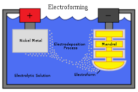
Electroforming for Precision Components
Nickel Sulphamate based plating solutions are employed wherever high speed, low stress, heavy nickel plating is required. The solutions are used for reclamation as well as for the production of moulds for plastics and rubber, filters, meshes and screens for the chemical, food, electronic and aircraft industry. In the printing industry nickel plating is employed for the facing of stereotypes and copper half tone plates in order to provide a hard wear-resistant surface and thus permit a very considerable increase in the number of impressions which can be obtained. Electro-types – duplicates of printing plates – are now generally electroformed in nickel rather than copper.
Electroforming is an extension of the electroplating process that enables the creation of solid nickel parts formed on a conductive template or mandrel. “E-formed” parts can be less than 25 microns (.001″) thick or up to 250 microns (.010″) thick. The process allows the creation of very fine details and structures. Particle sieves and nebulizer screens, micro-apertures for optronics and photonics are common applications for nickel electroforming.
By way of comparison, the practical limits for photochemical etching are 100 micron holes on 50 micron material and minimum 125 micron features on 125-micron or less material. Electroforming can produce foils less than 25 microns thick and holes under 10 microns. Generally speaking, in photo etching, feature sizes are driven by metal thickness. Holes must be at least 115% of the metal thickness, and land areas must be at least 90% of the metal thickness.